
Charger circuits for cell phones. Building a universal machine USB charger (attempt number one)
Most modern network chargers are assembled using a simple pulse circuit, using one high-voltage transistor (Fig. 1) according to a blocking generator circuit.
Unlike simpler circuits using a step-down 50 Hz transformer, the transformer for pulse converters of the same power is much smaller in size, which means the size, weight and price of the entire converter are smaller. In addition, pulse converters are safer - if in a conventional converter, when the power elements fail, the load receives a high unstabilized (and sometimes even alternating) voltage from the secondary winding of the transformer, then in case of any malfunction of the “pulse generator” (except for the failure of the reverse optocoupler) connection - but it is usually very well protected) there will be no voltage at the output at all.

Rice. 1
A simple pulse blocking oscillator circuit
A detailed description of the principle of operation (with pictures) and calculation of the circuit elements of a high-voltage pulse converter (transformer, capacitors, etc.) can be read, for example, in “TEA152x Efficient Low Power Voltage supply” at the link http://www. nxp.com/acrobat/applicationnotes/AN00055.pdf (in English).
The alternating mains voltage is rectified by diode VD1 (although sometimes the generous Chinese install as many as four diodes in a bridge circuit), the current pulse when turned on is limited by resistor R1. Here it is advisable to install a resistor with a power of 0.25 W - then if overloaded, it will burn out, acting as a fuse.
The converter is assembled on transistor VT1 according to the classic flyback circuit. Resistor R2 is needed to start generation when power is applied; in this circuit it is optional, but with it the converter works a little more stable. Generation is maintained thanks to capacitor C1, included in the PIC circuit on the winding, the generation frequency depends on its capacitance and the parameters of the transformer. When the transistor is unlocked, the voltage at the lower terminals of windings I and II in the diagram is negative, at the upper terminals it is positive, the positive half-wave through capacitor C1 opens the transistor even more strongly, the voltage amplitude in the windings increases... That is, the transistor opens like an avalanche. After some time, as capacitor C1 charges, the base current begins to decrease, the transistor begins to close, the voltage at the upper terminal of winding II in the circuit begins to decrease, through capacitor C1 the base current decreases even more, and the transistor closes like an avalanche. Resistor R3 is necessary to limit the base current during circuit overloads and surges in the AC network.
At the same time, the amplitude of the self-induction EMF through the diode VD4 recharges the capacitor SZ - that is why the converter is called flyback. If you swap the terminals of winding III and recharge the capacitor SZ during the forward stroke, then the load on the transistor will sharply increase during the forward stroke (it may even burn out due to too much current), and during the reverse stroke the self-induction EMF will be unspent and will be released by collector junction of the transistor - that is, it can burn out from overvoltage. Therefore, when manufacturing the device, it is necessary to strictly observe the phasing of all windings (if you mix up the terminals of winding II, the generator simply will not start, since capacitor C1 will, on the contrary, disrupt generation and stabilize the circuit).
The output voltage of the device depends on the number of turns in windings II and III and on the stabilization voltage of the zener diode VD3. The output voltage is equal to the stabilization voltage only if the number of turns in windings II and III is the same, otherwise it will be different. During the reverse stroke, capacitor C2 is recharged through diode VD2, as soon as it charges to approximately -5 V, the zener diode will begin to pass current, the negative voltage at the base of transistor VT1 will slightly reduce the amplitude of the pulses on the collector, and the output voltage will stabilize at a certain level. The stabilization accuracy of this circuit is not very high - the output voltage varies within 15...25% depending on the load current and the quality of the zener diode VD3.
A circuit of a better (and more complex) converter is shown in rice. 2

Rice. 2
Electrical circuit of a more complex
converter
To rectify the input voltage, a diode bridge VD1 and a capacitor are used; the resistor must have a power of at least 0.5 W, otherwise at the moment of switching on, when charging capacitor C1, it may burn out. The capacitance of capacitor C1 in microfarads must be equal to the power of the device in watts.
The converter itself is assembled according to the already familiar circuit using transistor VT1. A current sensor on resistor R4 is included in the emitter circuit - as soon as the current flowing through the transistor becomes so large that the voltage drop across the resistor exceeds 1.5 V (with the resistance indicated on the diagram being 75 mA), transistor VT2 opens slightly through diode VD3 and limits the base current of transistor VT1 so that its collector current does not exceed the above 75 mA. Despite its simplicity, this protection circuit is quite effective, and the converter turns out to be almost eternal even with short circuits in the load.
To protect transistor VT1 from emissions of self-induction EMF, a smoothing circuit VD4-C5-R6 was added to the circuit. The VD4 diode must be high-frequency - ideally BYV26C, a little worse - UF4004-UF4007 or 1 N4936, 1 N4937. If there are no such diodes, it is better not to install a chain at all!
Capacitor C5 can be anything, but it must withstand a voltage of 250...350 V. Such a chain can be installed in all similar circuits (if it is not there), including in the circuit according to rice. 1- it will noticeably reduce the heating of the switch transistor housing and significantly “extend the life” of the entire converter.
The output voltage is stabilized using the zener diode DA1 located at the output of the device, galvanic isolation is provided by the optocoupler V01. The TL431 microcircuit can be replaced with any low-power zener diode, the output voltage is equal to its stabilization voltage plus 1.5 V (voltage drop across the LED of the optocoupler V01)’; a small resistance resistor R8 is added to protect the LED from overloads. As soon as the output voltage becomes slightly higher than expected, current will flow through the zener diode, the optocoupler LED will begin to glow, its phototransistor will open slightly, the positive voltage from capacitor C4 will slightly open transistor VT2, which will reduce the amplitude of the collector current of transistor VT1. The instability of the output voltage of this circuit is less than that of the previous one and does not exceed 10...20%; also, thanks to capacitor C1, there is practically no 50 Hz background at the output of the converter.
It is better to use an industrial transformer in these circuits, from any similar device. But you can wind it yourself - for an output power of 5 W (1 A, 5 V), the primary winding should contain approximately 300 turns of wire with a diameter of 0.15 mm, winding II - 30 turns of the same wire, winding III - 20 turns of wire with a diameter of 0 .65 mm. Winding III must be very well insulated from the first two; it is advisable to wind it in a separate section (if any). The core is standard for such transformers, with a dielectric gap of 0.1 mm. As a last resort, you can use a ring with an outer diameter of approximately 20 mm.
This device was conceived a long time ago and was tested several times; everything presented below is the author’s development. Despite the very simple circuit, the device operates very stably. The device itself is a charger for a mobile phone without using wires.
How does all this work?
This device was published on this site. The first version turned out to be not very effective, then other versions were invented. This option turned out to be the most economical. The device allows you to charge a phone if the latter is located at a distance of no more than 3 - 4 cm from the receiver. The basis of the first device is a highly efficient PWM controller that can generate rectangular pulses with a frequency of up to 1 MHz, but due to large losses the idea turned out to be not very good, although this device allowed mobile devices to be charged at a distance of up to 50 cm from the receiver.
After some unsuccessful attempts to create such a device, a simplified blocking generator came to the rescue, which I successfully used in electroshock devices.
The main advantages of the device:
1) Low consumption
2) High efficiency (compared to its counterparts)
3) Relatively high charging current
4) Ability to operate from a reduced source (the first version operated from a voltage of 9-16 volts)
5) Simplicity and compactness
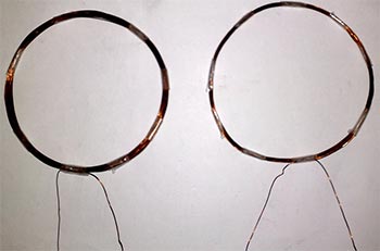
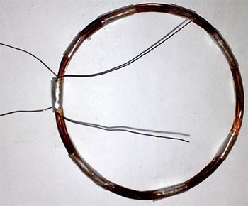
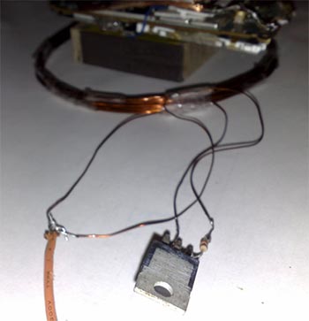
The transmitting part of the device consists of two main circuits. Each of them has a diameter of 10 cm, wound with 0.8 mm wire. The first circuit (L1) consists of 20 turns, the second of 35 turns of the same wire. The contours are laid on top of each other and decorated with adhesive tape or insulating tape.
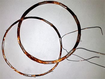
It is necessary to number the coil terminals in advance, since they need to be phased. They do phasing like this - the beginning of the first coil is connected to the end of the second or vice versa, the main thing is to get one coil with a tap.
Next, we select the resistance (if you plan to start the device from a reduced source, then the resistor can be removed).
It is advisable to use a trimming resistor of 0...470 Ohm; the power of the resistor is not very important (0.25-2 Watt).
How to set it up? Just! First, let's assemble the receiver circuit. We connect the power (any stabilized constant voltage source 4.5-9 volts). We adjust the resistor so that the quiescent current of the circuit does not exceed 150mA.
The maximum current consumption of the circuit is no more than 600mA, you will agree that this is not much.
After selecting the optimal resistance, you can replace the variable with a constant resistor (0.25-1W). The resistance of the basic limiter directly depends on the input voltage rating.
In my version, the transistor did not overheat, but just in case, install it on a small heat sink.
The device starts operating from a voltage of 1 volt - another feature of this design, but at this voltage it will not charge a mobile phone; instead, it can be used as a converter to power low-power devices.
Transistor - you can use literally any low-frequency transistor, regardless of structure. The circuit uses a KT818 transistor, which can be successfully replaced with 837, 816, 814 or 819, 805, 817, 815, only when using reverse conduction transistors, the power polarity should be changed.
Receiver
The design of the receiver is outrageously simple - a circuit, a rectifier, a zener diode and a storage capacitor. A pulse diode is needed, preferably in an SMD version, since the entire circuit will be located in a mobile phone. In my case, a fairly powerful and common Schottky diode SS14 was used. Such a diode is capable of operating at frequencies up to 1 MHz, the current is up to 1A!

The capacitor is not critical; it has a capacity from 47 to 220 µF (more is of course better, but there may not be enough space). Capacitor voltage is from 10 to 25 Volts.
Zener diode - any voltage of 5-6 volts (often found with a voltage of 5.6 Volts, for example - BZX84C5V6).

The receiver circuit (L3) contains 15 turns of 0.3-0.7 mm wire, wound in a spiral on the outer or inner side of the back cover of the phone.
The circuit can be assembled on a compact board or placed in a convenient place using hinged mounting, but it is advisable to fill the mounting with rubber glue or silicone.

A Sony Ericsson K750 was used as a test phone; it was fully working and was purchased specifically for these experiments (bought with spare parts for $5), then a handy Nokia N95 was converted.
The device can charge a mobile phone quite quickly, it all depends on the total power, in this case a 1000mA battery is fully charged in 3 hours.
The current is transmitted to the second circuit by electromagnetic induction, in this case it is completely safe, since the frequency is reduced, there are no harmful effects on humans.
In order to install the receiving circuit, the mobile phone is disassembled. An industrial charger is connected to the charging socket and the polarity is found on the socket contacts. Next, the receiver pins are connected to the corresponding pins of the socket.

The outline can be attached to the back cover of the phone using epoxy resin, silicone (highly not recommended), super glue (use only when the outline is planned to be attached to the outside of the cover).
List of radioelements
| Designation | Type | Denomination | Quantity | Note | Shop | My notepad |
|---|---|---|---|---|---|---|
| VT1 | Bipolar transistor | KT818A | 1 | KT837, KT816, KT814 | To notepad | |
| VD1 | Zener diode | BZX84C5V6 | 1 | 5-6 Volt | To notepad | |
| VD2 | Schottky diode | SS14 | 1 | To notepad | ||
| C1 | Electrolytic capacitor | 10 µF | 1 |
We looked at the circuit of a simple autonomous charger for mobile equipment, working on the principle of a simple stabilizer with lowering battery voltage. This time we will try to assemble a slightly more complex, but more convenient memory. The batteries built into miniature mobile multimedia devices usually have a small capacity, and, as a rule, are designed to play audio recordings for no more than several tens of hours when the display is turned off, or to play several hours of video or several hours of reading e-books. If a power outlet is unavailable or the power supply is turned off for a long period of time due to bad weather or other reasons, then various mobile devices with color displays will have to be powered from built-in energy sources.
Given that such devices consume considerable current, their batteries may be discharged before electricity is available from a wall outlet. If you do not want to immerse yourself in primitive silence and peace of mind, then to power your handheld devices you can provide a backup autonomous energy source, which will help out both during a long journey into the wild, and in case of man-made or natural disasters, when your settlement may be on the verge of destruction. several days or weeks without power supply.

Mobile charger circuit without 220V network
The device is a linear voltage stabilizer of the compensation type with a low saturation voltage and a very low intrinsic current consumption. The energy source for this stabilizer can be a simple battery, rechargeable battery, solar or manual electric generator. The current consumed by the stabilizer when the load is off is about 0.2 mA at an input supply voltage of 6 V or 0.22 mA at a supply voltage of 9 V. The minimum difference between the input and output voltage is less than 0.2 V at a load current of 1 A! When the input supply voltage changes from 5.5 to 15 V, the output voltage changes by no more than 10 mV at a load current of 250 mA. When the load current changes from 0 to 1 A, the output voltage changes by no more than 100 mV at an input voltage of 6 V and by no more than 20 mV at an input supply voltage of 9 V.
A self-resetting fuse protects the stabilizer and battery from overload. The reverse-connected diode VD1 protects the device from reverse polarity of the supply voltage. As the supply voltage increases, the output voltage also tends to increase. To maintain the output voltage stable, a control unit assembled at VT1, VT4 is used.
An ultra-bright blue LED is used as a reference voltage source, which, while performing the function of a micro-power zener diode, is an indicator of the presence of output voltage. When the output voltage tends to increase, the current through the LED increases, the current through the emitter junction VT4 also increases, and this transistor opens more, and VT1 also opens more. which bypasses the gate-source of the powerful field-effect transistor VT3.
As a result, the resistance of the open channel of the field-effect transistor increases and the voltage across the load decreases. Trimmer resistor R5 can be used to adjust the output voltage. Capacitor C2 is designed to suppress self-excitation of the stabilizer as the load current increases. Capacitors C1 and SZ are blocking capacitors in the power supply circuits. Transistor VT2 is included as a micro-power zener diode with a stabilization voltage of 8..9 V. It is designed to protect against high-voltage breakdown of the gate insulation of VT3. A gate-source voltage that is dangerous for VT3 may appear when the power is turned on or due to touching the terminals of this transistor.
Details. The KD243A diode can be replaced by any of the KD212, KD243 series. KD243, KD257, 1N4001..1N4007. Instead of KT3102G transistors, any similar ones with low reverse collector current are suitable, for example, any of the KT3102, KT6111, SS9014, BC547, 2SC1845 series. Instead of the KT3107G transistor, any of the KT3107, KT6112, SS9015, VS556, 2SA992 series will do. A powerful p-channel field-effect transistor of the IRLZ44 type in a TO-220 package, has a low gate-source opening threshold voltage, a maximum operating voltage of 60 V. The maximum constant current is up to 50 A, the open channel resistance is 0.028 Ohm. In this design, it can be replaced with IRLZ44S, IRFL405, IRLL2705, IRLR120N, IRL530NC, IRL530N. The field-effect transistor is installed on a heat sink with a cooling surface area sufficient for a particular application. During installation, the terminals of the field-effect transistor are short-circuited with a jumper wire.

The autonomous charger can be mounted on a small printed circuit board. As an autonomous power source, you can use, for example, four pieces of series-connected alkaline galvanic cells with a capacity of 4 A/H (RL14, RL20). This option is preferable if you plan to use this design relatively rarely.

If you plan to use this device relatively often or your player consumes significantly more current even when the display is off, then it would be advisable to use a 6 V rechargeable battery, for example, a sealed motorcycle battery or from a large hand-held flashlight. You can also use a battery of 5 or 6 nickel-cadmium batteries connected in series. When hiking, fishing, to recharge batteries and power a handheld device, it may be convenient to use a solar battery capable of delivering a current of at least 0.2 A with an output voltage of 6 V. When powering the player from this stabilized energy source, it should be taken into account that the regulating transistor is turned on into the negative circuit, therefore, simultaneous power supply of the player and, for example, a small active speaker system is only possible if both devices are connected to the output of the stabilizer.
The purpose of this circuit is to prevent a critical discharge of the lithium battery. The indicator turns on the red LED when the battery voltage drops to a threshold value. The LED turn-on voltage is set to 3.2V.

The zener diode must have a stabilization voltage lower than the desired LED turn-on voltage. The chip used was 74HC04. Setting up the display unit involves selecting the threshold for turning on the LED using R2. The 74NC04 chip makes the LED light up when the discharge reaches the threshold that will be set by the trimmer. The current consumption of the device is 2 mA, and the LED itself will light up only at the moment of discharge, which is convenient. I found these 74NC04 on old motherboards, so I used them.
PCB:


To simplify the design, this discharge indicator may not be installed, because the SMD chip may not be found. Therefore, the scarf is specially placed on the side and can be cut along the line, and later, if necessary, added separately. In the future I wanted to put an indicator on the TL431 there, as a more profitable option in terms of details. The field-effect transistor is available with a reserve for different loads and without a radiator, although I think it is possible to install weaker analogues, but with a radiator.


SMD resistors are installed for SAMSUNG devices (smartphones, tablets, etc., they have their own charging algorithm, and I do everything with a reserve for the future) and they can not be installed at all. Do not install domestic KT3102 and KT3107 and their analogues; the voltage on these transistors was floating due to h21. Take BC547-BC557, that's it. Source of the diagram: Butov A. Radio constructor. 2009. Assembly and adjustment: Igoran .
Discuss the article MOBILE CHARGING FOR YOUR PHONE
The number of mobile communications devices in active use is constantly growing. Each of them comes with a charger supplied in the kit. However, not all products meet the deadlines set by the manufacturers. The main reasons are the low quality of electrical networks and the devices themselves. They often break down and it is not always possible to quickly purchase a replacement. In such cases, you need a phone charger circuit, using which it is quite possible to repair a faulty device or make a new one yourself.
Main faults of chargers
The charger is considered the weakest link in mobile phones. They often fail due to poor-quality parts, unstable mains voltage or as a result of ordinary mechanical damage.
The simplest and best option is to purchase a new device. Despite the differences in manufacturers, the general schemes are very similar to each other. At its core, this is a standard blocking generator that rectifies the current using a transformer. Chargers may differ in connector configuration, they may have different circuits of input network rectifiers, made in a bridge or half-wave version. There are differences in small things that are not of decisive importance.
As practice shows, the main faults of the memory are the following:
- Breakdown of the capacitor installed behind the mains rectifier. As a result of the breakdown, not only the rectifier itself is damaged, but also a constant resistor with low resistance, which simply burns out. In such situations, the resistor practically acts as a fuse.
- Transistor failure. As a rule, many circuits use high-voltage high-power elements marked 13001 or 13003. For repairs, you can use the domestically produced KT940A product.
- Generation does not start due to a breakdown of the capacitor. The output voltage becomes unstable when the zener diode is damaged.
Almost all charger housings are non-separable. Therefore, in many cases, repairs become impractical and ineffective. It is much easier to use a ready-made DC source by connecting it to the required cable and supplementing it with the missing elements.
Simple electronic circuit
The basis of many modern chargers are the simplest pulse circuits of blocking generators, containing only one high-voltage transistor. They are compact in size and capable of delivering the required power. These devices are completely safe to use, since any malfunction leads to a complete absence of voltage at the output. This prevents high unstabilized voltage from entering the load.

The rectification of the alternating voltage of the network is carried out by the diode VD1. Some circuits include an entire diode bridge of 4 elements. The current pulse is limited at the moment of switching on by resistor R1 with a power of 0.25 W. In case of overload, it simply burns out, protecting the entire circuit from failure.
To assemble the converter, a conventional flyback circuit based on transistor VT1 is used. More stable operation is ensured by resistor R2, which starts generation at the moment of power supply. Additional generation support comes from capacitor C1. Resistor R3 limits the base current during overloads and power surges.
High reliability circuit
In this case, the input voltage is rectified by using a diode bridge VD1, a capacitor C1 and a resistor with a power of at least 0.5 W. Otherwise, while charging the capacitor when turning on the device, it may burn out.
Capacitor C1 must have a capacity in microfarads equal to the power of the entire charger in watts. The basic circuit of the converter is the same as in the previous version, with transistor VT1. To limit the current, an emitter with a current sensor based on resistor R4, diode VD3 and transistor VT2 is used.

This phone charger circuit is not much more complicated than the previous one, but much more efficient. The inverter can operate stably without any restrictions despite short circuits and loads. Transistor VT1 is protected from emissions of self-induction EMF by a special chain consisting of elements VD4, C5, R6.
It is necessary to install only a high-frequency diode, otherwise the circuit will not work at all. This chain can be installed in any similar circuits. Due to this, the housing of the switch transistor heats up much less, and the service life of the entire converter increases significantly.
The output voltage is stabilized by a special element - a zener diode DA1, installed at the charging output. Optocoupler V01 is used.
DIY charger repair
With some knowledge of electrical engineering and practical skills in working with tools, you can try to repair a cell phone charger on your own.
First of all, you need to open the charger case. If it is dismountable, you will need an appropriate screwdriver. With the non-separable option, you will have to use sharp objects, separating the charge along the line where the halves meet. As a rule, a non-separable design indicates low quality chargers.

After disassembly, a visual inspection of the board is carried out in order to detect defects. Most often, faulty areas are marked with traces of burning resistors, and the board itself will be darker at these points. Mechanical damage is indicated by cracks in the case and even on the board itself, as well as bent contacts. It is enough to bend them back into place towards the board to resume the supply of mains voltage.
Often the cord at the output of the device is broken. Breaks most often occur near the base or directly at the plug. The defect is detected by measuring resistance.
If there is no visible damage, the transistor is desoldered and ringed. Instead of a faulty element, parts from burnt-out energy-saving lamps are suitable. Everything else was done - resistors, diodes and capacitors - are checked in the same way and, if necessary, replaced with serviceable ones.
I wonder what the Siemens charger (power supply) consists of and whether it is possible to repair it yourself if it breaks.
First, the block needs to be disassembled. Judging by the seams on the body, this unit is not intended for disassembly, therefore it is a disposable item and you don’t have to place much hope in the event of a breakdown.

I literally had to tear apart the body of the charger; it consists of two tightly glued parts.

Inside is a primitive circuit board and several parts. The interesting thing is that the board is not soldered to the 220V plug, but is attached to it using a pair of contacts. In rare cases, these contacts may oxidize and lose contact, leaving you thinking the unit is broken. But I was pleasantly pleased with the thickness of the wires going to the connector for the mobile phone; you don’t often see a normal wire in disposable devices; usually it is so thin that it’s scary to even touch it).
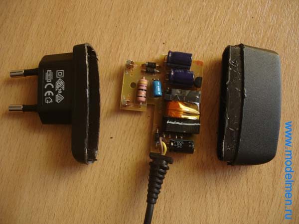
There were several parts on the back of the board; the circuit turned out to be not so simple, but still not so complicated that you couldn’t fix it yourself.

Below in the photo are the contacts of the inside of the case.

There is no step-down transformer in the charger circuit; its role is played by an ordinary resistor. Next, as usual, a couple of rectifying diodes, a pair of capacitors for rectifying the current, then comes a choke and finally a zener diode with a capacitor completes the chain and outputs the reduced voltage to a wire with a connector to the mobile phone.

The connector has only two contacts.
